This video shows how to assign a solution setup for a cut out subdesign of the Intel Galileo board and then perform post processing operations after simulati. Ansys hfss 3d layout tutorial Ansys HFSS.

Lecture 4 Hfss 3d Layout Middot Pdf Filelecture 4 Hfss 3d Layout Introduction To Ansys Hfss Ndash Select The Menu Item Layout Draw Hfss Air Box Ndash Select
View this demonstration of how to create Vias with Ansys HFSS 3D Layout.
. Hfss 3d layout design tutorial Written By cucchiaro Friday March 18 2022 Add Comment Edit The modifications from the original design are smaller antenna and lowering the impedance with one director the same principle is used. To create an analysis setup select the menu item HFSS Analysis Setup Add Solution Setup. De ne variables HFSS Design Properties add r pad 075 mm t pad 01 mm as the radius and the thickness of the via pad respectively.
Ease-of-use drive 3D simulation for design engineers Layout-Driven Assembly in ANSYS Electronics Desktop Apply automated circuit simulation to capture full system behavior Place and connect components in Layout Simulate components with 3D accuracy ECAD and MCAD HFSS SIwave Q3D. Full-wave frequency-domain 3-D field solver based upon finite element method. Antenna design and platform integration Filters and waveguide.
From a layout generate layer by layer 2D triangular mesh. As what I understood from your explanation you have design antenna for 24 Ghz. 7 ADD Frequency Sweep.
Start All Programs ANSYS Electromagnetics HFSS 150 Windows 64-bit or 32-bit HFSS 150 Set HFSS options. It supports various layout formats generated in other major ECAD systems for analysis using the HFSS solver. HFSS 3D Layout only Pro.
This tutorial demonstrates how to create a 3D Component from an existing HFSS model of a connector and add it to a target design which is a printed circuit. HFSS Tutorials for Beginners to Professionals. Em_ Talk - HFSS Tutorial 1_ Microstrip Patch Antenna - Free download as PDF File.
Overview of HFSS. Insert a New Design Project-Insert HFSS Design. HFSS - 3D Layout Guides.
Initial Mesh 16x 850k tets 1. Problem Description Getting Started Create the 3D model Analysis Setup Plot S-parameters vs. 1 full torrent Ansoft HFSS v11.
Sweep mesh in stackup z direction to generate tetrahedral mesh elements Advantage. Tianjian Lu ECE 546. The Ansys HFSS 3D Layout course for printed circuit board design focuses on layered structures using the 3D Layout design type in HFSS and AEDT Ansys Electronic Desktop.
In the Solution Setup window click the general tab Solution frequency is 255 GHz Maximum Number of Passes is 20 and Maximum Delta S per Pass is 002. Adaptive Mesh 12x 1. 156m 2019 R1 Flow Improvements HFSS Layout 3D with Mesh Assembly Faster initial mesh time Faster user experience Non-graphical.
I have done the design using HFSS 3D Design environment where I individually created each layer and stacking them manually about 40 layers total. I am trying to design a stackup layer consisting of metals and dielectrics in HFSS. It is analogous to the terminal solution type in HFSS.
Enhanced Meshing in HFSS 3D Layout ¼ of multilayer flip-chip package. Only works for stack-up or swept in Z geometries. HFSS in 3D Layout provides.
As you can imagine this was very time consuming about 6 hours. 4m Layout w Mesh Assembly. Hfss 3d Layout Design Tutorial SIwave的circuit port與HFSS 3D Layout的circuit port還是有些不同前者是SPICE type後者是Field type 有較大的寄生電感效應.
Energol hlp 46 msds design of triangular patch antenna using hfss. Layout w Mesh Assembly. Direct Import of Cadence mcm brd sip files and ODB Layout intelligent Automatic Port Setup Support circuit ports of SIwave Industry Leading Meshing capacity Advanced Phi mesher reduces 30 40x Parameterized Stackup Geometry Solve at DC with integrated DC solver.
Ansys hfss 3d layout tutorial Ansys HFSS. Tools Options HFSS Options General Tab Check Use Wizards for data input when creating new boundaries Check Duplicate boundariesmesh operations with geometry Click OK. If this is my correct.
HFSS 3D Layout generates. Industry-standard accuracy Adaptive meshing of arbitrary geometry Fully parametric modeling Optimization and HPC Multi-physics via Ansys Workbench. Intro to Ansys HFSS 3D Layout Lesson 1.
This workshop covers the simulation aspects of ESD board modeling in HFSS 3D layout and its analysis. This lesson introduces the tool and covers the interface details. HFSS 3D Classic 5hrs 15min HFSS 3D Layout w Classic v15 3hrs 41 min HFSS 3D Layout meshing advantages Mesh and solve non-manifold geometry Mesh geometries with large aspect ratios Layer-based geometry is easier to edit modify clean up etc.
And its has given desired results. Workshops include a small. Resonance frequency but it is resonating at 27 Ghz.
Avoid setting a gap port with long length to minimize the parasitic inductance. The outline for this workshop is as follows. This webinar series shows you how the HFSS adaptive meshing technology handles massive PCB layout geometries and gives you the most.
How to Create Vias for Simulation within HFSS. Extremely fast relative to classic 3D mesh approach Con. 186m 144GB RAM 2.
如何在HFSS 3D佈局中構建和模擬微帶線HFSS 3D Layout是平面佈局設計環境 我們需要首先定義基板的疊層然後在每層上構建佈局. Widely used for RFmicrowave design. Gap port is like the lump port you knew in HFSS before.
Both is on TOP layer and the reference ground is at Layer 4. Skips heavyweight ACIS and 3D surface mesh generation Availability. Im trying to define 2 waveport over 2 differential nets.
It is a bit different than the HFSS 3D CAD. Restore archive file comprising setup and analysis validate the design analyze the design view the results. Designed for brand new users this course covers layer stackup layout viewing ports vias simulation boundary extents layout driven assembly and hierarchy.
Ansys HFSS 3D layout is a design type within the Ansys HFSS product. Layout w Mesh Assembly. Now you need to identify your analysis setup.

Ansys Hfss 3d Layout Model From A Cadence Board File Youtube
Hfss 3d Layout Hfss教程

How To Build And Simulate Microstrip In Hfss 3d Layout Youtube
Ansys Hfss 3d Layout Cut Out Sub Design Simulation And Post Processing Youtube

How To Define Electronics System In Hfss 3d Layout Youtube

Hfss 3dlgs Tsne Ws2 1 Tracelayer Pages 1 10 Flip Pdf Download Fliphtml5

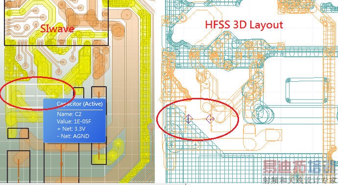
How To Model Vias Of High Speed Differential Pairs With Hfss In Siwave Simulation Youtube

Transient Time Domain Solutions From Hfss 3d Layout Youtube
0 comments
Post a Comment